
SMT fasteners PCB high-current conductive connection
PCB Solder Standoffs / Nut Columns
Product photos
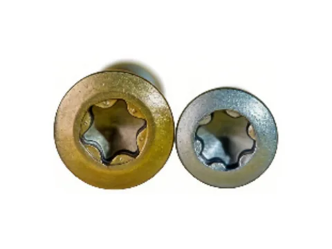
Actual photos, not renders
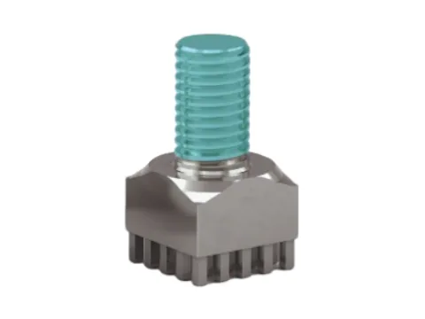
Illustration note
The image shows an actual part of this specification; appearance differs with surface treatment and head style, and the delivered part prevails.
Images are for appearance and structure reference; dimensions and tolerances are subject to the specifications and the applicable standards on this page.
Product description
Compiled from the existing technical description of this product on this site
PCB high-current terminals are designed for high-current scenarios and soldered onto the PCB, using high-conductivity copper alloy to provide a low-resistance, high-current electrical connection. The conductive cross-section is enlarged and the heat dissipation path optimized to ensure stable and reliable power transmission in high-power circuits, suitable for power, drive and power-conversion boards.
Specifications
The parameters listed on this page are subject to final inspection and the applicable standards; items not listed follow the customer drawing or the order agreement and are not committed by default.
| Material | Copper alloy (high conductivity) |
|---|---|
| Process | Welded fastening |
| Surface treatment | Tin plating / nickel plating |
| Standard | Per customer drawing / company standard; electrical performance testing per GB/T 5095 |
| Typical application | PCB high-current conductive connection |
Spec lookup
Based on your operating conditions, look up directly among the 8 models in this series — pure front-end filtering, no redirects, no URL changes
Filter results are based on the specification fields published on each model page and are for preliminary screening only; the final selection must be confirmed in light of the actual load, plate thickness and assembly process.
Drawings & customization
No public catalogue is available for this series; drawing-based requests are handled per project.
Made to drawing / sample replication
A 2D drawing or a physical sample is enough for evaluation; once confirmed, we issue drawings, build samples and obtain first-article approval before volume production. Drawings and project information are handled under confidentiality requirements.
Manufacturing process
The usual process route for this product family; actual operations follow the drawing and order requirements.
- Precision turning / cold headingPan head and thread forming
- End-face and thread machiningFlatness control of the mounting surface
- ElectroplatingMatte tin / nickel plating, reflow-compatible
- Tape packagingCompatible with SMT placement equipment
- Full inspection of dimensions and platingPlacement and soldering compatibility verification
Capacity & delivery
Taken from the company's published capacity and certification information; no unverified claims are included.
FAQ
Material, standards, surface treatment and installation points for this model; the data comes from the specification table on this page and from the national standards cited in the answers.
Q1What material is the PCB high-current terminal made of? What strength level does it achieve?
Materials listed in the specification table on this page: copper alloy (high conductivity). Material certificates and mechanical property test reports can be provided with delivery; batch acceptance follows the above specifications.
Q2What surface treatments are available for the PCB high-current terminal? How to choose?
Surface treatment listed in the specification table on this page: tin plating / nickel plating. Different platings differ in appearance, corrosion resistance and cost; choose according to the service environment and the order agreement.
Q3Which applications is the PCB high-current terminal suitable for?
Typical applications listed in the product description on this page: power and inverter boards; EV drive control boards; industrial variable-frequency and servo drives; high-power LED and charging modules. Overview: PCB high-current terminals are designed for high-current scenarios and soldered onto the PCB, using high-conductivity copper alloy to provide a low-resistance, high-current electrical connection.
Q4What manufacturing process is used for the PCB high-current terminal?
Process listed in the specification table on this page: solder fixing. The process route follows the drawings and order requirements; first-article approval is provided before volume production.
Q5What electrical performance requirements apply to conductive parts such as the PCB high-current terminal?
Copper-alloy conductive parts are made to drawing with controlled contact resistance and plating; electrical performance testing refers to the GB/T 5095 series of methods. When used for grounding or shielding, attention should also be paid to contact reliability after the plating oxidizes. (Applies to this model, PCB high-current terminal.)
Related models
Alternative sizes in the same series and cross-series fasteners commonly used together
SMT fasteners
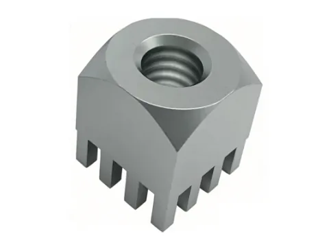
PCB High-Current Terminal 1
High-current crimp terminal, made of selected high-conductivity alloy with a precision cold-heading process and a special electroless plating; contact resistance is extremely low, suitable for high-power connections
SMT fasteners
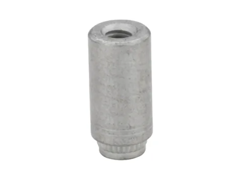
1.2mm PCB Internal/External Thread Super Screw
PCB solder standoff, made of free-cutting steel or copper alloy, tin-plated to optimize solderability. A precision locating step at the base

SMT fasteners
SMT nut
SMT tape & reel fasteners, packaged in carrier tape conforming to EIA standards
Direct Assembly
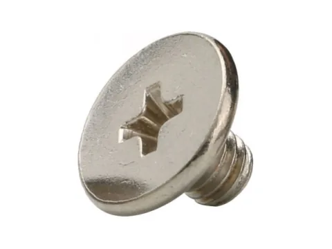
0.6 mm CM Phillips Ultra-Thin Ultra-Short Large-Head Micro Screw
A 0.6 mm ultra-thin large-head design that pushes space utilisation to the limit, effectively increasing the contact area and preventing the sheet from being pierced. Precision Phillips drive combined with a very short thread body.
Insert Screws
TORX PLUS Insert Screws
Made of class 12.9 high-strength alloy steel